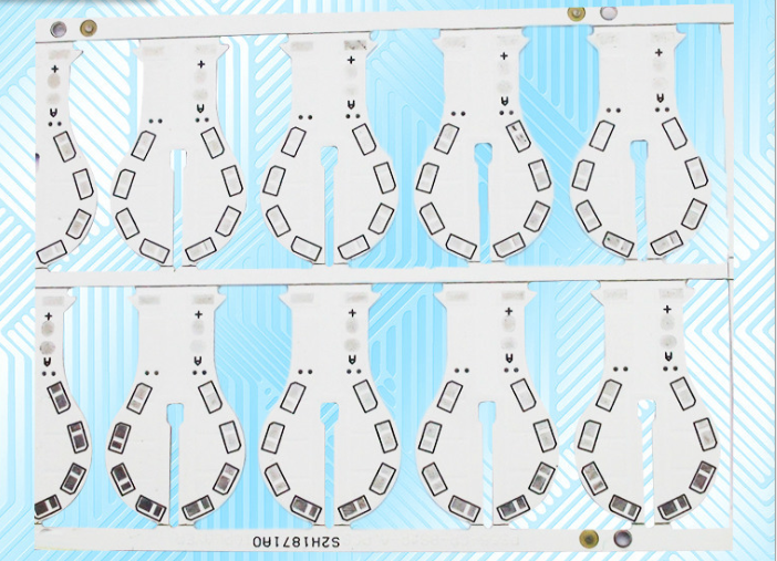
V2 Plate PCB Printed Circuit Board Double Sided Fiberglass Cloth
Substrate
Capability
| 1 | High precision prototype | PCB bulk production |
2 | 1-28 layers | 2 layers |
| 3 | 3mil | 2mil |
| 4 | 0.15mm | 1.6mm |
| 5 | Aspect Ration≤13:1 | Aspect Ration≤13:1 |
| 6 | 2 layers:0.2mm;4 layers:0.35mm;6 layers:0.55mm;8 layers:0.7mm;10
layers:0.9mm | 1 layers |
| 7 | Immersion Gold:Au,1—8u”
Gold finger:Au,1—150u”
Gold Plated:Au,1—150u”
Nickel Plated :50—500u” | Nickel Plated :50—500u” |
| 8 | Board thickness≤1.0mm:+/-0.1mm
1.0mm<Board thickness≤2.0mm:+/-10%
Board thickness>2.0mm:+/-8% | Board thickness≤1.0mm |
| 9 | ≤100mm:+/-0.1mm
100< ≤300mm:+/-0.15mm
>300mm:+/-0.2mm | ≤100mm:+/-0.1mm |
| 10 | ±10% | 5% |
Mechanical Layer
The Protel 99 SE provides 16 mechanical layers, which are used to
set the dimensions,
data marks, alignment marks, assembly instructions and other
mechanical information of
the board.This information may vary depending on the requirements
of the design company
or PCB manufacturer.Can perform menu commands Design |
MechanicalLayer circuit boards
set more mechanical layer.In addition, the mechanical layer can be
attached to other
layers together with the output display.
Solder mask layer
Apply a coat of paint, such as antisolder paint, to all areas
outside the pad to prevent
tin from being applied to these areas.The solder resistance layer
is used to match pads
during the design process and is automatically generated.The Protel
99 SE provides two
Solder resistance layers: Top Solder and Bottom Solder.
Paste mask layer(SMD layer)
It acts in a similar way to the solder barrier, except for the
corresponding surface -
bonded component pads during machine soldering.Protel99 SE provides
Top Paste and Bottom
Paste protection layers.
It is mainly aimed at the SMD components on PCB board.If the board
is full of DIP
(through-hole) components, there is no need to output Gerber files
on this layer.Before
the SMD components are pasted on the PCB board, the solder Paste
must be applied on each
SMD solder pad. In the steel mesh used for tin coating, the Paste
Mask file must be used
to process the film.
The most important thing to be clear about the Gerber output of
Paste Mask layer is that
this layer is mainly for SMD components. At the same time, compare
this layer with the
Solder Mask introduced above to understand the different functions
of the two layers,
because the two film pictures are very similar from the film
pictures.
Keep out layer
Use to define areas on a board where components and wiring can be
placed
efficiently.Draw a closed area on this layer as a valid area for
cabling. Automatically
layout and cabling cannot be done outside this area.
7 Silkscreen Layer 7 Silkscreen Layer
The screen printing layer is mainly used to place printed
information, such as the
outline and annotation of components, various annotation
characters, etc.The Protel 99
SE provides Top Overlay and Bottom Overlay for screen printing.In
general, all kinds of
annotation characters are in the top layer of screen printing, the
bottom layer can be
closed.
Multi Layer
The solder pads and through-holes on the circuit board need to
penetrate the whole
circuit board to establish an electrical connection relationship
with different
conductive graphic layers, so the system is specially set up an
abstract layer -
multilayer.Generally, the pads and holes should be set on multiple
layers. If this layer
is closed, the pads and holes will not be shown.
Drill Layer
The borehole layer provides drilling information during the
fabrication of the circuit
board (e.g. solder pads, which require drilling to pass through
holes).The Protel 99 SE
provides two Drill beds, DrillGride and Drill Drawing.


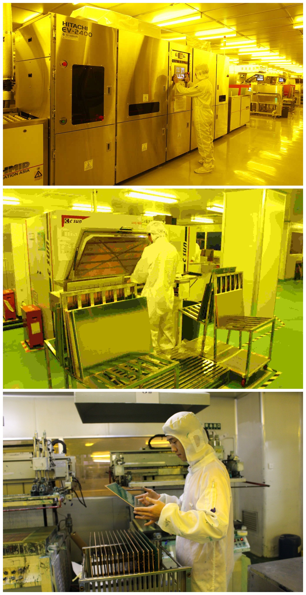
Ping You Industrial Co.,Ltd
Ping You Industrial Co.,Ltd is a professional and reliable one-stop PCB solutions provider for
customers specialized in manufacturing quick turn prototypes and
small volumes.Topfast is responsible for overseas business
development.With high quality and on-time delivery products we won
the market's wide acclaim. We will continue to focus on customer
satisfaction, along with "high quality "and "fast delivery", we
will become a PCB service provider worthy of customer trust.